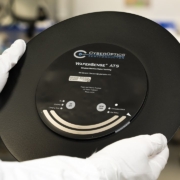
 Used Auto Leveling Sensor (ALS) WaferImprove equipment setup time
Enhance process uniformity with objective and reproducible level adjustments
Reduce equipment maintenance time with wireless measurement
Reduce particles and increase yield with improved equipment set-up
Wafer-shaped: Available in 200mm and 300mm wafer sizes
Highly accurate: Measures horizontal leveling
Wireless: Transmits data wirelessly to your laptop or PC in real-time
Data logging: Records raw data in CSV format for analysis
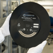
 Used Auto Vibration Sensor (AVS) WaferSpeed equipment qualification with wireless vibration measurements
Shorten equipment maintenance cycles with a wafer-like accelerometer
Lower equipment expenses with objective and reproducible data
Optimize equipment productivity and yield by maximizing acceleration and minimizing vibration
Wafer-shaped: Available in 200mm and 300mm wafer sizes
Highly accurate: Measures acceleration in three directions. x, y and z. with a range of +/-2G, resolution of +/-0.01G and frequency response 0 to 200 Hz, -3dB
Wireless: Transmits data to your laptop or PC in real-time (CSV raw data also available)
Easy-to-use software: CyberSpectrum software provides the user with real-time visual feedback and can record and replay logged data for review and analysis
 Used Auto Teach System (ATS) Camera WaferAccurate wafer handoff calibration improves yield and lowers particulate contamination.
WaferSense ATS wafer moves through your semiconductor equipment just as a wafer to capture offset data for accurate
calibration of transfer positions.
Wireless communications and wafer form factors reduce equipment downtime from hours to minutes.
Wireless and vacuum compatible, the ATS teaching wafer makes calibration safe for both technicians and
process stations.
Visual inspection speeds up troubleshooting and lowers consumable expenses.
ATS displays real-time images to technicians as robots move ATS through the tool.
 Used Auto Gapping System (AGS) WaferImprove uniformity and yield with wireless gap measurement wafer
Achieve chamber matching and parallelism in a very short timeMeasures gaps at three points or five points to allow you to achieve the ideal leveling and platen/showerhead parallelism for your CVD equipment Objective and reproducible gap adjustments result in better tool-to-tool process uniformity
Take the human variable out of adjusting your equipment with objective (numerical) measurements. Numerical and graphical
displays make adjustments fast and simple.CyberSpectrum software, the graphical user interface provided with AGS, displays numerical and graphical measurements in either
millimeters or inches from inside the process chamber under a vacuum, letting you see the effect of your adjustments in real-time.
Wireless technology eliminates broken wires and vacuum leaks.
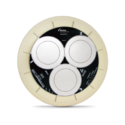
 Used Airborne Particle Sensor (APS) WaferDetect particles in real-time without opening the tool, so you don’t need to expose process areas to the environment. The APS wafer is used for rapid tool partitioning and segmentation.
Reports particles in 0.14μm and 0.5μm bin sizes and larger particles in 2, 5, 10 and 30 μm bin sizes.
Available in 150mm, 200mm, and 300mm wafer sizes.
Transmits particle data to your laptop or PC in real-time.
CyberSpectrum application software provides the user with real-time visual feedback and can record and replay logged data for review and analysis.
Raw data also saved in CSV format for analysis.

